Reverse Engineering PCB Tips for 2026 Canton Fair Buyers?
The 2026 Canton Fair presents a unique opportunity for buyers to explore innovative products, especially in advanced manufacturing and electronics. One area gaining interest is "Reverse Engineering Pcb." This method involves analyzing printed circuit boards to understand their design and functionality.
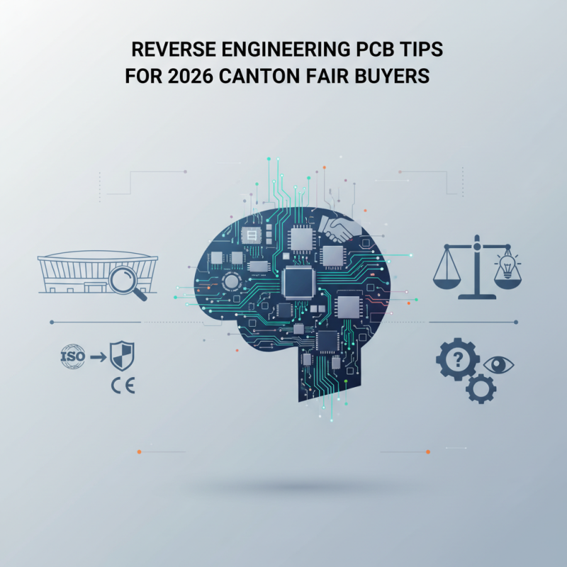
Visitors can leverage the fair's AI features to find suppliers who specialize in PCB technology. With a focus on certifications like ISO and CE, buyers can ensure quality while navigating through the sprawling 155,000 square meters of exhibition space. Yet, amid this vast selection, the challenge remains: how to discern the truly innovative offerings from mere replicas.
Engaging in Reverse Engineering PCB can raise ethical questions. Buyers should reflect on the implications of using such techniques. Understanding the balance between innovation and integrity is essential. The Canton Fair not only showcases products but also encourages dialogue on responsible sourcing in electronics.
Essential Tools for Reverse Engineering PCBs at the Canton Fair
Reverse engineering PCBs is becoming critical for manufacturers seeking innovation. Understanding component placement and circuit pathways requires precision tools. By 2025, the global PCB market is expected to reach $80 billion, emphasizing the importance of reverse engineering during trade events like the Canton Fair.
Key tools include high-resolution microscopes and multi-meters. A good microscope allows for close inspection of solder joints. This can reveal design flaws or manufacturing shortcuts. Multi-meters help verify component functionality. This process can expose potential issues with third-party products, leading to improved designs.
However, reverse engineering is not without challenges. Tools can be expensive, and learning curves may be steep. Maintaining ethical standards is crucial. Using these insights can lead to better products but demands careful reflection on processes. Ultimately, the right tools can guide manufacturers toward smarter investments and enhanced quality.
Understanding PCB Design and Layout Before the Canton Fair
Understanding PCB design is crucial for anyone attending the Canton Fair. It helps buyers make informed decisions. A well-designed PCB can significantly impact product performance. Poor design choices can lead to issues. Think about component placement, trace width, and grounding. These details may seem minor, yet they affect functionality.
Layout considerations also play a vital role. Ensure the design adheres to industry standards. This avoids complications during the manufacturing process. If a layout is cluttered, signal integrity may suffer. Clean layouts facilitate easier troubleshooting. However, balancing complexity and simplicity can be challenging. Many designers wrestle with this balance.
Finally, don't overlook the importance of testing. Simulate your PCB design before final production. Testing reveals potential flaws early on. Addressing these flaws early saves time and resources. Buyers should critically evaluate samples during the fair. Learning from past mistakes in designs can lead to better future purchases.
Reverse Engineering PCB Tips for 2026 Canton Fair Buyers
| Aspect | Details |
| PCB Types | Single-sided, Double-sided, Multi-layer |
| Common Materials | FR-4, CEM-1, Polyimide |
| Design Software | Altium Designer, Eagle, KiCad |
| Manufacturing Process | Etching, Drilling, Layer Lamination |
| Common Components | Resistors, Capacitors, ICs |
| Testing Methods | Functional Testing, In-Circuit Testing |
| Regulatory Compliance | RoHS, CE, UL |
| Design Considerations | Signal Integrity, Thermal Management, Layout Guidelines |
Common Challenges in Reverse Engineering PCBs and Solutions
Reverse engineering printed circuit boards (PCBs) presents various challenges, particularly for those attending events like the 2026 Canton Fair. One major issue is component identification. Understanding the purpose of each component is crucial. Many designs use similar parts. Distinguishing one from another can be frustrating. This requires patience and attention to detail.
Another common challenge is the layout mapping. The arrangement of components on a PCB can be complex. Replicating these layouts often leads to inaccuracies. Even professionals struggle with nuances in design. It’s easy to overlook small traces or vias. Having a systematic approach to document each layer is essential. Often, users find themselves retracing steps, which can be time-consuming.
Lastly, software tools can create hurdles. Choosing the right software for analysis is vital. Not all tools support every file type. Compatibility issues surface frequently. Users may experience crashes or freezes during crucial moments. This can lead to loss of valuable time. Reflecting on these challenges can lead to better strategies when tackling PCB reverse engineering at trade shows.
Best Practices for Documenting PCB Reverse Engineering Findings
When diving into PCB reverse engineering, documentation is key. Clear notes can guide your findings and help others understand your process. It’s important to capture your observations promptly. Use diagrams and photographs to create a visual record. These elements enhance comprehension and detail.
Here are some tips to improve your documentation. Organize your findings chronologically. This method makes it easier to track your progress. Highlight key components and any challenges you encounter. Don't shy away from noting areas of confusion or unexpected results. These reflections can lead to important insights later.
Consider using digital tools for better organization. Apps and software can streamline your documentation process. However, there’s a risk of overcomplicating things. Keep your recording methods simple yet effective. Always ask yourself if your notes serve their purpose. This level of scrutiny will refine your understanding and process.
Networking Opportunities at the Canton Fair for PCB Professionals
Attending the Canton Fair in 2026 offers vast networking opportunities for PCB professionals. Meeting industry experts is crucial. Engaging in discussions can unveil new insights into PCB design and manufacturing. These conversations often lead to collaborations. However, making the right connections can be overwhelming.
To navigate this, consider attending workshops and seminars during the fair. These sessions focus on reverse engineering techniques. You can interact with speakers and ask questions. This direct engagement could lead to mentorship opportunities. Yet, don’t hesitate to approach companies of interest. Carry your portfolio to demonstrate your skills. Remember, not every interaction will be successful, and that’s okay.
Be prepared for informal networking too. Casual coffee breaks can turn into valuable discussions. Don't overlook the importance of social events. Here, you might meet potential collaborators outside business settings. However, managing time effectively is crucial. Balance between formal meetings and informal chats can be challenging. Refine your approach and learn from past experiences. Networking may not yield quick results, but the relationships formed are often worth the effort.
PCB Reverse Engineering Trends - Canton Fair 2026